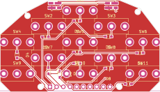
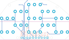
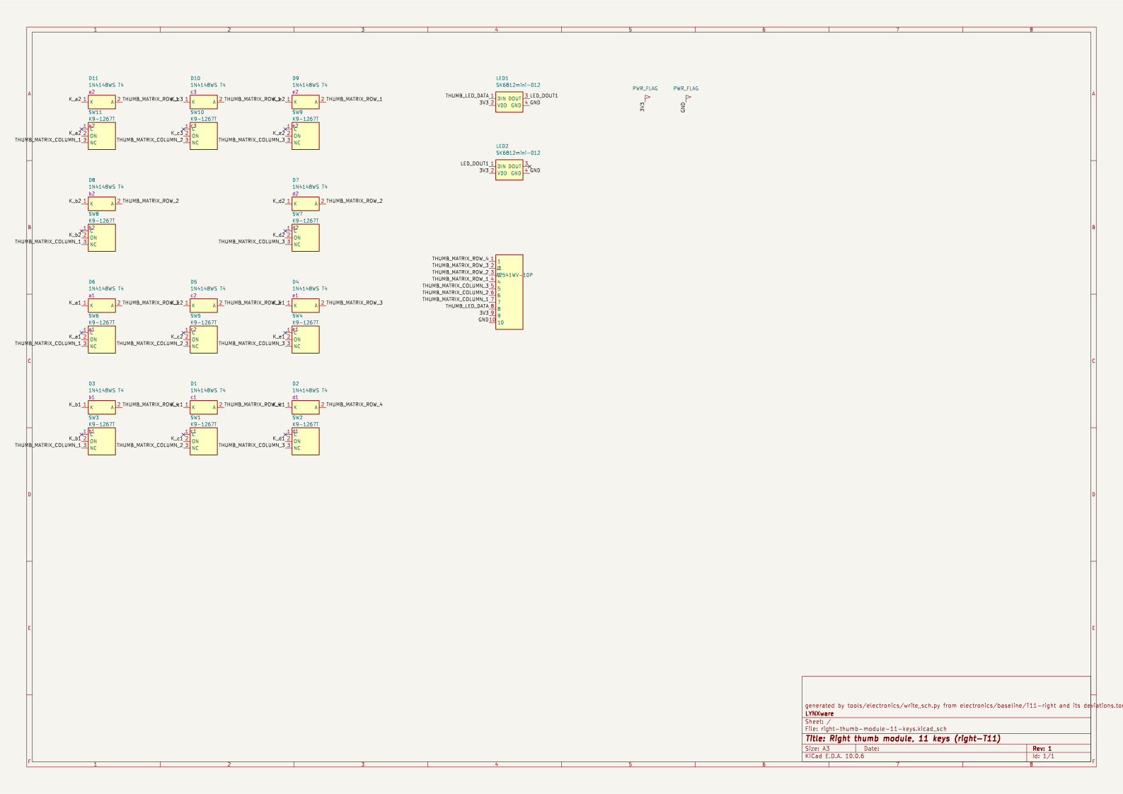
Right thumb module, 11 keys (right-T11) — 2 LEDs
Redrawn in KiCad from its EasyEDA Pro source like left-T11, through the
qualification gate. Source of truth: this KiCad project
since the gate was ticked on 2026-09-25. The frozen export
(ProPrj_CAT-v4_Thumb_Right_Keys-11_2026-08-01.epro2 in the private EasyEDA archive, board
Thumb_Right_Keys-11_v0.4.0_1) is the archived original. Generated from
electronics/baseline/T11-right/ with its deviations: placed and routed,
with the source's copper except around the two LEDs.
The board mirrors left-T11: switches and holes exactly, the header pin order reversed
(wiring-harness.toml). J1 is a different 1×10 header part than the left's (A2541WV-10P, C225485),
kept as in the source.
Differences from the source
Decided, dated and checked exactly by check_board.py (deviations.toml):
LED1,LED2: SK6812mini-012 instead of WS2812B-Mini (one LED part on both thumbs, 2026-09-24), pins mapped by function.- Their centres and orientation mirror left-T11's
U1/U2, under the mirrored cover's light windows (2026-09-25); the source's LEDs were up to 0.6 mm off that mirror. - The copper at both LEDs (2026-09-25): the SK6812's pins sit in other corners, so 18 source traces and 2 vias are replaced by 20 traces and 4 vias. The data line now crosses the supply at LED1 and ground at LED2, each once through the bottom layer. At LED1 the 3V3 trace runs over the data-out pad, 0.23 mm from it and 0.28 mm from the board edge. All other 111 traces and 5 vias are the source's.
Resolved by construction, no deviation needed: the signal nets the source left auto-named
($1N…) carry their names through wiring-harness.toml net_aliases; the outline, drawn as two open
polylines in the source, is one closed polygon (the reader stitches it).
Gate record (2026-09-25)
| Step | State | Evidence |
|---|---|---|
| Archive the original export | ✅ | sha256 14c01913…db22d204 |
| Produce the KiCad project | ✅ | generated, deterministic, saved by kicad-cli 10.0.6 |
| Resolve symbols, footprints, 3D models | ✅ | check_lib.py right-T11; the project's own library since 2026-09-26 (electronics/lib/README.md), copper unchanged |
| Schematic ↔ PCB association, parity | ✅ | pcb drc --schematic-parity: no entry |
| Diff connectivity | ✅ | 61 connected pads, 22 nets, both directions, against baseline ∘ deviations |
| Diff placement | ✅ | every pad within 0.01 mm; LEDs at the mirrored left-T11 positions |
| Diff outline, holes | ✅ | 60.96 × 35.0 mm, 10 vertices, closed; 4 holes Ø2.0 |
| Keys vs the Assembly | ✅ | 11 cells |
| Connector labels | ✅ | the signals' silk aliases from wiring-harness.toml |
| Diff copper | ✅ | 131 traces and 9 vias exactly as baseline ∘ deviations; the GND pour on the source's polygon; every net one piece, DRC 0 unconnected items |
| ERC / DRC | ✅/⚠️ | 0 errors; four source edge pads as warnings (below); inherited silkscreen warnings |
| Human review | ✅ | Stas, in KiCad 10.0.6, 2026-09-25, including the new LED copper |
Findings
- Outer switch pads touch the board edge, mirrored from left-T11:
SW4/SW9pad 1 andSW6/SW11pad 3 at 0.000 mm. Named inright-thumb-module-11-keys.kicad_dru. - The outline is close to, not exactly, the mirror of left-T11's: the upper corners differ by fractions of a millimetre, and one corner has a single vertex where the left has two. Kept as the source has it; worth one look against the mirrored cover.
- The connector label
LED_DATA(the wiring harness alias ofTHUMB_LED_DATA) is longer than the source'sTdataand runs up towards the switch pads; the fab clips silk over pads. D4,D7,D9(the diodes turned 90°) were placed reversed by the first redraw (commit f02226e) — see left-T11 finding 5; fixed.
Hand-over
Edit this board in KiCad from now on, as left-T11 describes.