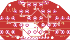
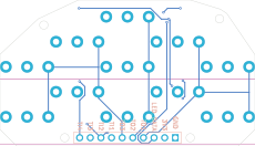
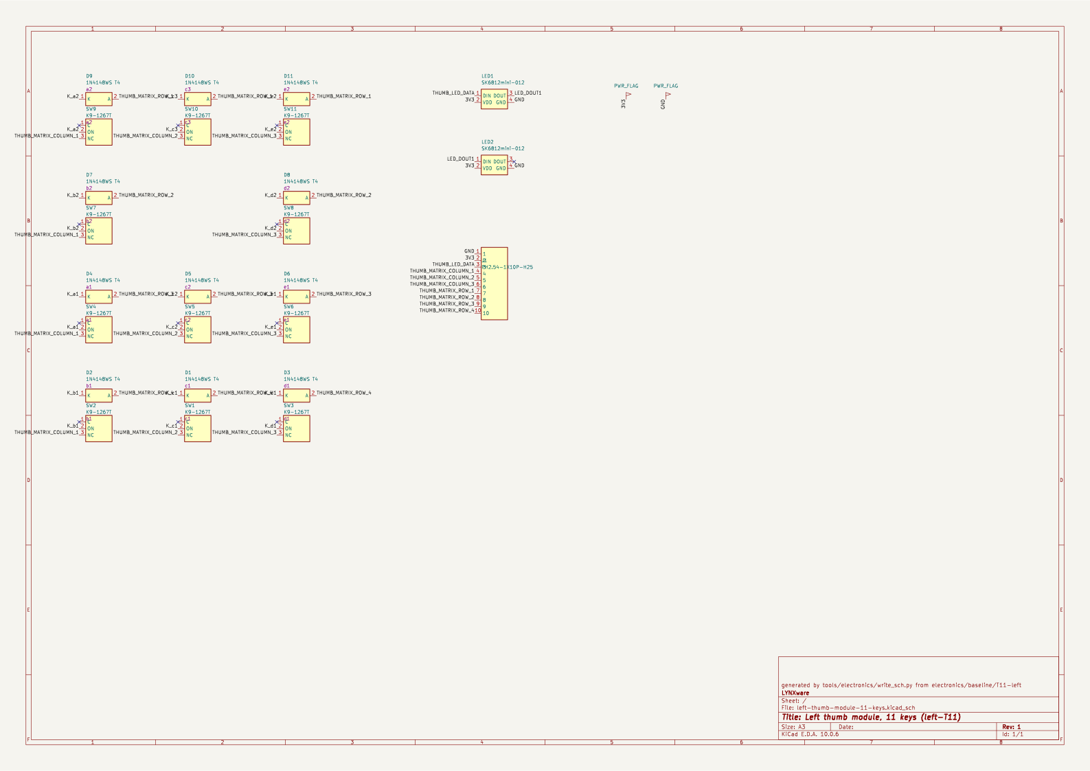
Left thumb module, 11 keys (left-T11) — 2 LEDs, the pilot board
The first board redrawn in KiCad from its EasyEDA Pro source, netlist-driven, through the
qualification gate. Source of truth for this board: this
KiCad project since the gate was ticked on 2026-09-25. The frozen export
(ProPrj_CAT-v4_Thumb_Left_Keys-11_2026-08-01.epro2 in the private EasyEDA archive, board
left_thumb-module_keys_v0.4.0_1, PCB PCB_L-T-k_1) is the archived original. The KiCad files
were generated from electronics/baseline/T11-left/, placed and routed with the source's
copper, trace for trace, the GND pour on top filled by KiCad. No deviations from the source.
Gate record (2026-09-25)
| Step | State | Evidence |
|---|---|---|
| Archive the original export | ✅ | private EasyEDA archive, sha256 6ced7394…047e17 |
| Produce the KiCad project | ✅ | generated, deterministic (uuid5), saved by kicad-cli 10.0.6 |
| Resolve symbols, footprints, 3D models | ✅ | electronics/lib/ (check_lib.py left-T11: all pads match; the SOD-323 pad width is an accepted difference in lib/parts.toml); the project's own library since 2026-09-26, copper unchanged |
| Schematic ↔ PCB association, parity | ✅ | footprints carry path to their symbol; pcb drc --schematic-parity: no entry |
| Diff connectivity | ✅ | check_board.py: 61 connected pads, 22 nets, identical net classes in schematic and board vs the baseline, both directions; 12 no-connects match the baseline's open pads |
| Diff pad numbering, polarity | ✅ | pad ↔ net per pad number, and every source trace ends on the pad of its own net (DRC: no short, nothing unconnected) — the diode's anode/cathode and the LED's DIN/DOUT follow from it |
| Diff placement | ✅ | every pad of every footprint within 0.01 mm of the baseline's absolute pad position (orientation and side solved from the pads, not assumed) |
| Diff outline, holes, layers | ✅ | outline bbox 60.96 × 35.0 mm and 11 vertices; 4 holes at the baseline positions; 2 copper layers |
| Connector labels | ✅ | every header pad labelled with its wiring-harness.toml signal's silk alias (TI1…, LED_DATA) at the source's label position |
| Diff copper | ✅ | all 147 source traces and 11 vias at their source position, width and net; the GND pour on the source's rectangle; every net one piece (GND through the filled pour), DRC 0 unconnected items |
| ERC | ✅ | 0 errors, 0 warnings (./lx pcb check left-T11 --routed) |
| DRC | ✅/⚠️ | 0 errors; copper-to-edge held to 0.2 mm, the four source pads below reported as warnings by left-thumb-module-11-keys.kicad_dru; one dangling track end (finding 4); silkscreen warnings inherited from the library footprints |
| Manufacturing outputs vs the last ordered package | n/a | no package recovered (electronics/README.md) |
| Human review | ✅ | Stas, in KiCad 10.0.6, 2026-09-25 |
Findings while redrawing
- Outer switch pads touch the board edge.
SW4/SW9pad 3 andSW6/SW11pad 1 (the outer pads of the outer columns, x = ±29.08 mm, Ø2.8 mm pads) are tangent to the outline at x = ±30.48 — 0.0 mm copper-to-edge, in the source too; JLCPCB asks 0.2 mm on a routed edge. Named inleft-thumb-module-11-keys.kicad_dru; a before-next-order item. - The K9-1267T is used on pins 2 and 3 with pin 1 open, reproduced from the pad ↔ net
table; the datasheet check of
electronics/docs/before-next-order.mdstill applies. - Silkscreen: the pulled footprints' silk overlaps between the diode and switch outlines and runs over pads (the DRC warnings). Cosmetic; the source had the same.
- The source has a 0.26 mm stub of
LED_DOUT1running pastLED2pad 1 to nowhere (DRCtrack_dangling). Reproduced; harmless, removable on review. D6,D8,D11(the diodes turned 90°) were placed reversed by the first redraw (commit f02226e): the generators rotated footprints clockwise where KiCad turns them counter-clockwise, and the placement check shared that error. The source's traces exposed it; fixed intools/electronics/layout.py.
Hand-over
Edit this board in KiCad from now on. The generators refuse to overwrite a routed board
(--force would discard the KiCad edits); place_from_baseline.py left-T11 --silk-only still
refreshes the connector labels, and check_board.py left-T11 --routed shows what an edit
changed against the source.