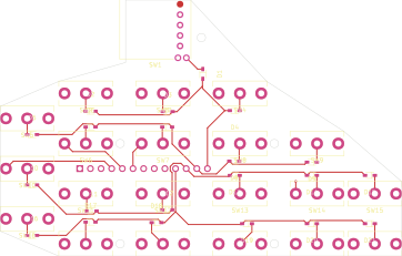
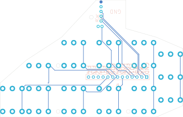
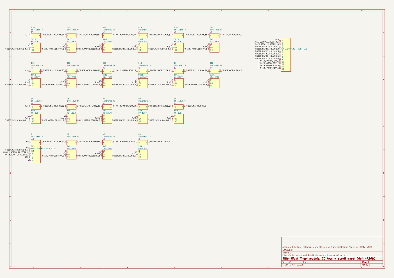
Right finger module, 20 keys + scroll wheel (right-F20W)
Redrawn in KiCad from its EasyEDA Pro source like left-T11, through the
qualification gate. Source of truth: still the frozen
export (ProPrj_CAT-v4_Finger_Right_Keys-20+Wheel_2026-08-01.epro2 in the private EasyEDA archive,
board Right-Finger-KeysWheel-Variante2, PCB PCB_R-F-KWv2) until the gate is ticked.
Generated from electronics/baseline/F20w-right/: placed and routed with the source's
copper, trace for trace. No deviations from the source.
Parts: SW1 is the EVQWGD001 scroll-wheel encoder. Its push switch sits on cell (3,0), the
m0 position with its own diode D1, where the left board fits a plain key; its Key field
is m0, its canonical path right.fingers.wheel.click, and its A/B/C pins carry FINGER_SCROLL_ENCODER_A, FINGER_SCROLL_ENCODER_B (silk WA, WB) and GND.
SW2…SW21 are the K9-1267T keys with D2…D21. J1 the 1×13 header (C2932703) on the bottom.
No pour.
Gate record (2026-09-25)
| Step | State | Evidence |
|---|---|---|
| Archive the original export | ✅ | sha256 0a8d2c59…9d5ff34b |
| Produce the KiCad project | ✅ | generated, deterministic, saved by kicad-cli 10.0.6 |
| Resolve symbols, footprints, 3D models | ✅ | check_lib.py right-F20W; the project's own library since 2026-09-26 (electronics/lib/README.md), copper unchanged; the encoder's body since 2026-10-02, drawn from a reference model |
| Schematic ↔ PCB association, parity | ✅ | pcb drc --schematic-parity: no entry |
| Diff connectivity | ✅ | 100 connected pads, 34 nets, both directions |
| Diff placement | ✅ | every pad within 0.01 mm |
| Diff outline, holes | ✅ | 95.885 × 61.256 mm, 11 vertices; 5 holes Ø2.0 |
| Keys vs the Assembly | ✅ | 21 cells, the wheel button as m0 |
| Connector labels | ✅ | the signals' silk aliases from wiring-harness.toml: pin 9 now reads FO6 (FINGER_MATRIX_COLUMN_6; the source's Fo9 was wrong) |
| Diff copper | ✅ | all 171 source traces and the via at their source position, width and net; every net one piece, DRC 0 unconnected items |
| ERC / DRC | ✅/⚠️ | 0 errors; five source edge pads as warnings (below); inherited silkscreen warnings |
| Human review | ⏳ | Stas, in KiCad |
Findings
- Outer switch pads cross the board edge, as on left-F21:
SW5,SW10,SW16pad 3 by 0.033 mm,SW15,SW21pad 1 by 0.042 mm. Named inright-finger-module-20-keys-scroll-wheel.kicad_dru. - The encoder footprint has a Ø1.6 mm copper disc without a drill, on both copper layers, 2.5 mm below pad 6 (an EasyEDA multi-layer fill). Reproduced as the source has it. ❓ If it was meant as the hole for the encoder's positioning boss, it must become a Ø1.6 NPTH before the next order. Panasonic publishes no drawing; the reference model the encoder's body is drawn from puts a Ø1.3 boss, 1.2 mm long, on the disc, and the open-source EVQWGD001 footprints drill Ø1.5–1.7 NPTH there. Check it on a part.
- The encoder's pad 6 is unconnected in the source (
lib/README.md). D1(the one diode turned 90°) was placed reversed by the first redraw (commit f02226e) — see left-T11 finding 5; fixed.
Hand-over
⚠️ Stas: open right-finger-module-20-keys-scroll-wheel.kicad_pro in KiCad 10.0.6 and review; "Update PCB from Schematic"
should report no change. Then tick "Human review".