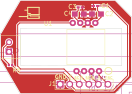
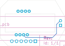
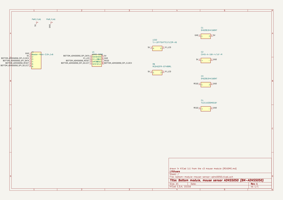
Bottom module, mouse sensor ADNS-5050 (BM-ADNS5050) — the v3 mouse module, drawn 1:1
Drawn in KiCad, not redrawn from a frozen EasyEDA source: this KiCad project is the board's only
source (authority drawn_in_kicad), and its "Human
review" tick below gates its release. The board is the v3 one, kept as it is (decided
2026-10-16): same outline, parts, placement and copper, no holes added. Its lid holds it in a
pocket.
Where it comes from
The v3 EasyEDA Standard export PCB_PCB_adns5050_2026-10-16.json (sha256
0a9460a0…53b179, kept outside the repository: it carries LCSC library records), converted
once from its 10 mil unit by a throwaway script. Origin: the source's canvas origin, which is
U1's origin and lies on the board's long axis; x points to the chamfered end, the header is on +y.
- Outline 35.00 × 25.00 mm, symmetric about y = 0: x −22.30 (the pointed end, at the LED) to 12.70 (the chamfered end), y ±12.50.
- Cutout 26.95 × 9.9 mm, from x −16.95 to 10.00, under the sensor and on to the LED: v3 drew it as an unplated region of the sensor's footprint; here it is a second Edge.Cuts polygon, its four corners as v3 has them (the end at the LED is 0.08 mm out of square). The sensor looks down through it, as Avago mounts it: body on the component side, its lens (ADNS-5100-001) under the board, the LED's leads bent 90° into the lens's clip (ADNS-5050 datasheet, figures 3–5).
- Parts, all on the top side, with v3's designators: U1 the ADNS-5050; LED2 a 5 mm red LED,
anode (pad 1, square) on 5 V, cathode on
XY_LED; R6 499 Ω across it (Avago's Ropt); C1 100 nF and C2 4.7 µF on 5 V, C3 100 nF and C4 3.3 µF onREGO, the sensor's regulator output (the datasheet's figure 8); J1 the 1×6 header, H1 on v3 (J, as on every module board). Pads are v3's; parts and links:electronics/lib/parts.toml. - Copper v3's 16 tracks (49 segments), 0.254 mm, one of them on the back (
XY_LED, U1 to LED2), and its ground pour on the front over the whole board, filled by KiCad (v3's clearance and spokes, 0.254 mm).GNDreaches the header only through the pour. - Silkscreen v3's header labels, its circle beside U1 pin 4 (the corner of Avago's logo) and its small drawing in the corner above LED2; the footprints' own outlines are the library's.
Header
| J1 pin | Net | Main-board pin (harness [breakouts.bm-adns5050]) | v3 silkscreen |
|---|---|---|---|
| 1 (square) | GND | 22, GND | GND |
| 2 | 5V | 21, 5V: USB only | V |
| 3 | BOTTOM_ADNS5050_SPI_CLOCK | 20, GPIO14 | sclk |
| 4 | BOTTOM_ADNS5050_SPI_DATA | 19, GPIO13 | sdio |
| 5 | BOTTOM_ADNS5050_RESET | 18, GPIO12 | n |
| 6 | BOTTOM_ADNS5050_SPI_SELECT | 17, GPIO11 | nsc |
These are v3's pins: the header meets six main-board pins in a row, pin 1 on 22, so one straight
6-wire cable joins them. The harness holds each header pin to its signal by its row, so
./lx pcb check holds no header pin to a signal here.
Before ordering
- LED polarity. v3 wires pad 1 (square) to 5 V, so the LED's anode, its long lead, goes in the square pad; check that against the v3 module that ran.
- The sensor is discontinued (
build.tomladns5050-moduletodo), as are its lens and clip. - Silkscreen (DRC warnings, not errors): LED2's outline runs off the pointed end, as the LED overhangs it on v3; C4's and J1's designators, at v3's positions, touch a pad and J1's outline in KiCad's wider font.
Check record (2026-10-16)
| Step | State | Evidence |
|---|---|---|
| Symbols, footprints, 3D models | ✅ | electronics/lib (write_lib.py --check); pads from the v3 board, outlines and the sensor's model from Avago's and the parts' drawings; LED2 has no model (no_model: the clip places it) |
| ERC | ✅ | 0 errors, 0 warnings |
| DRC with schematic parity | ✅/⚠️ | 0 errors, no parity entries, 0 unconnected items; warnings: the silkscreen above |
| Pad ↔ net against v3 | ✅ | all 26 pads within 1 µm of v3's and on its nets (v3's U1_n named after the sensor's pin), checked once by the drawing script |
| Assembly | n/a | fitted to no slot, no keys |
| Human review | ⏳ | Stas, in KiCad |
How it was drawn
Generated once from the v3 JSON (parts, outline, cutout, tracks, pour, silkscreen) with a
throwaway script, then saved and filled by KiCad 10.0.6. From here on, edit it in KiCad; there is
no generator to rerun. ./lx pcb check BM-ADNS5050 --routed gates it.